
Empowering Innovation: Our Advanced Resources
Explore the state-of-the-art technologies and services driving breakthrough development at OcuVista Solutions.
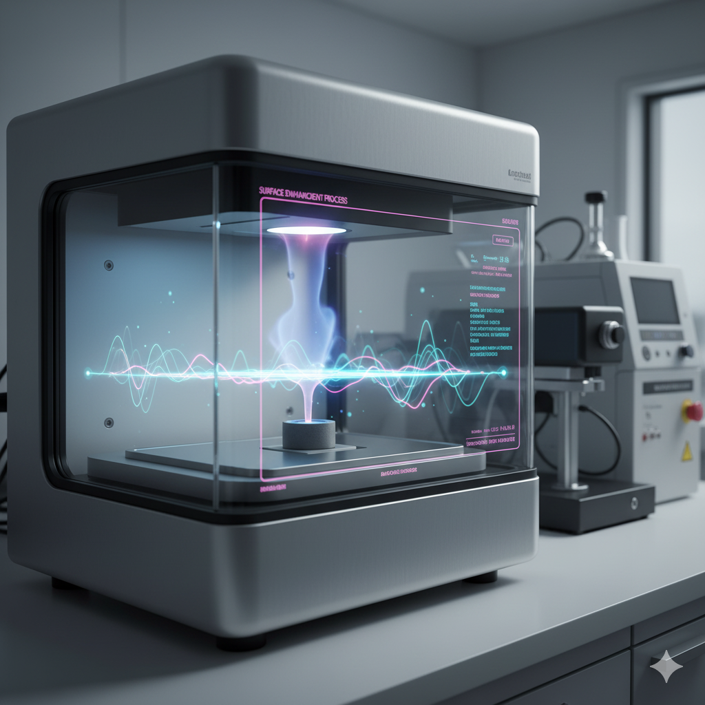
Low Pressure Plasma Surface Modification System
Harnessing plasma technology to enhance material surfaces for optimal performance.
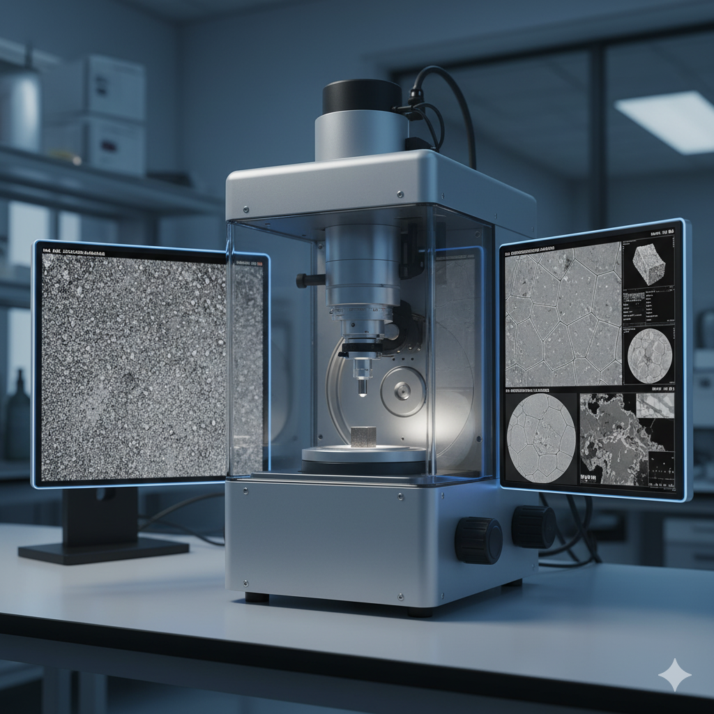
Scanning Electron Microscopy (SEM)
High-resolution imaging to explore material structures at the microscale.

Transmission Electron Microscopy (TEM)
Ultra-detailed imaging and analysis at the atomic level for scientific insights.

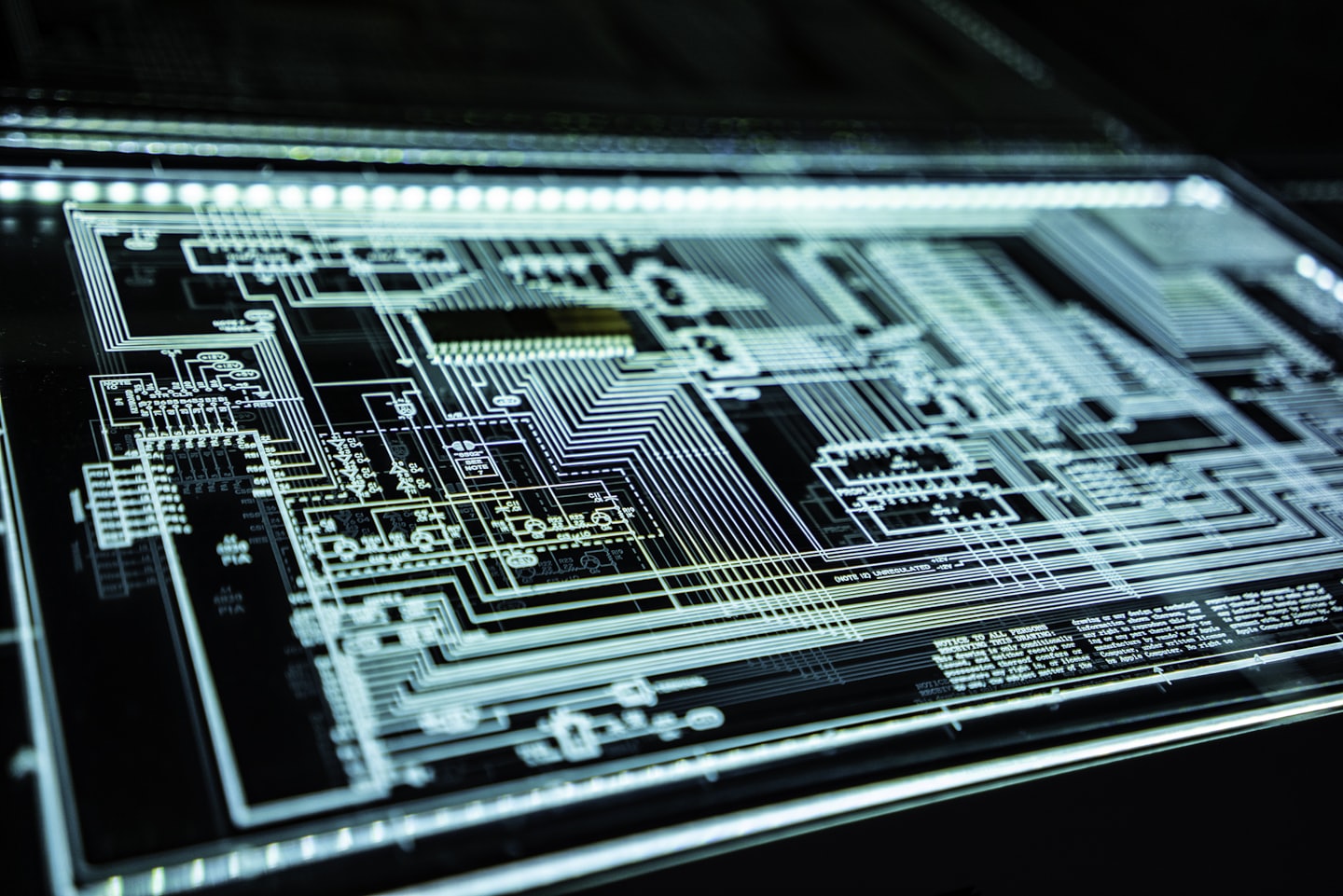
X-ray Photoelectron Spectroscopy
Advanced chemical characterization for surface and elemental analysis.
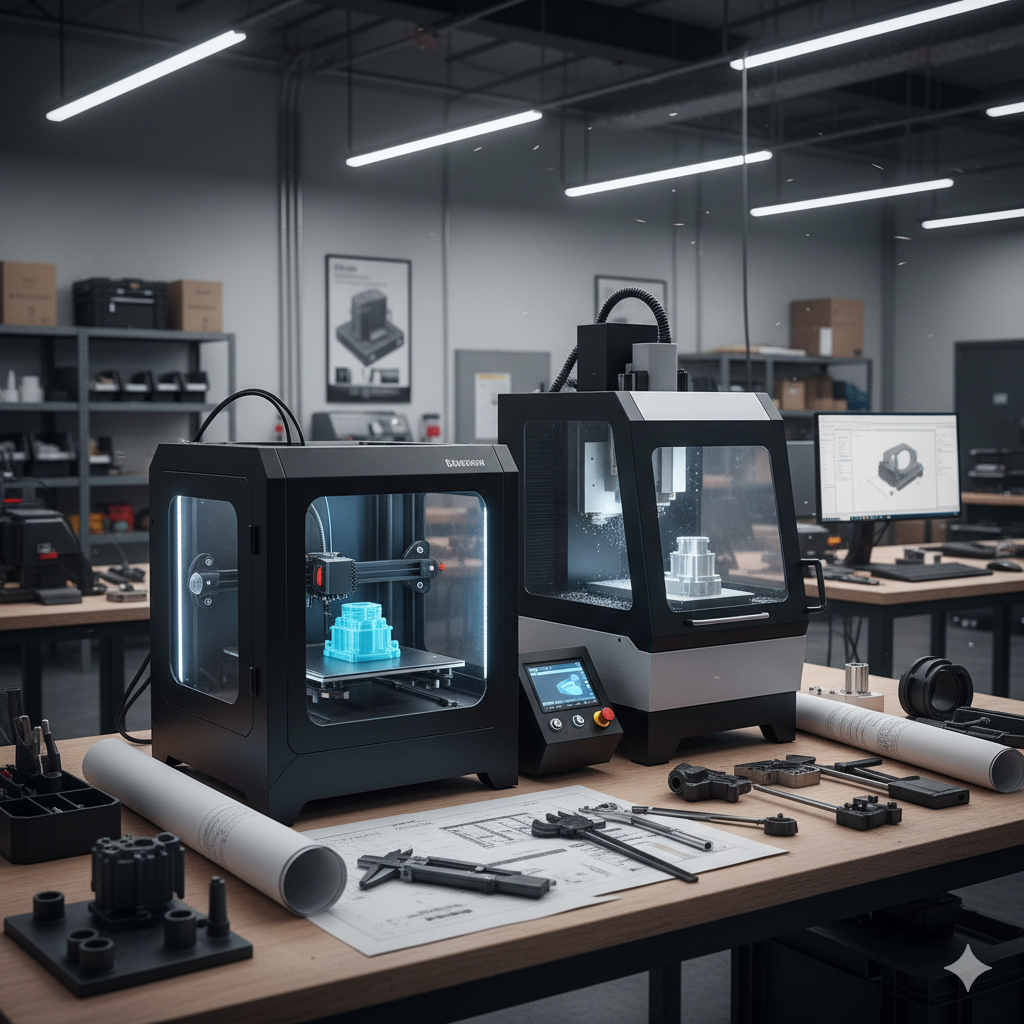
Prototyping Services
Rapid design and fabrication turning concepts into functional prototypes.
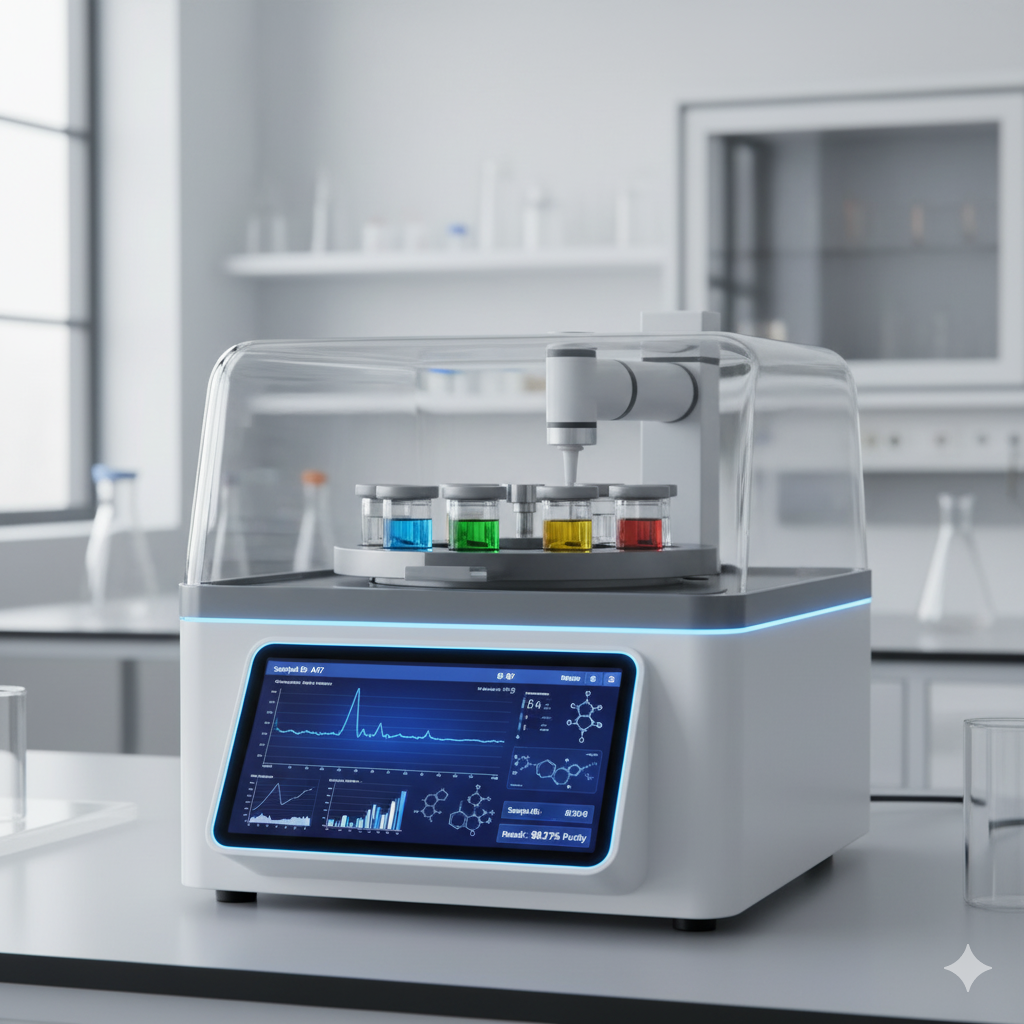
Chemical Detection and Analysis
Precision instruments for identification and measurement of chemical compositions.
Frequently Asked Questions
Find quick answers about OcuVista Solutions’ technologies, services, and support.
What types of solutions does OcuVista offer?
OcuVista delivers deep tech innovations in material science, medtech, and applied consumer technologies.
How can OcuVista Solutions improve my technical products?
Our innovative tools and software streamline optical processes and enhance visual performance.
Are OcuVista’s products compatible with existing materials?
Yes—our solutions are designed for seamless integration with a wide range of industry-standard materials.
Where can I get support for OcuVista products?
Access our dedicated support team through the Contact Us page or schedule a consultation for tailored assistance.
Our Process
Discover how OcuVista Solutions transforms your material and technology performance with our clear, guided approach.
1
Step One: Create Prototype(s) on your sample materials
From Concept to Reality: Tailored Prototyping on Your Materials
2
Step Two: Stress Testing
Pushing Boundaries: Rigorous Testing for Performance & Durability
3
Step Three: Optimize and Enhance
Refine and Advance: Maximizing Potential Through Data-Driven Enhancement